Silicon carbide (SIC) is a new generation of "energy-saving components" that have attracted much attention in the industry because of their advantages such as low power loss, high withstand voltage resistance, and smaller size, which can make machines energy-saving, miniaturized, and efficient. With the continuous development of society, the third generation of semiconductor materials will be widely used in home appliances and consumer electronics, new energy vehicles, industry and other high-tech fields, with broad market prospects, and the third generation of semiconductor era represented by silicon carbide and gallium oxide is also coming
|
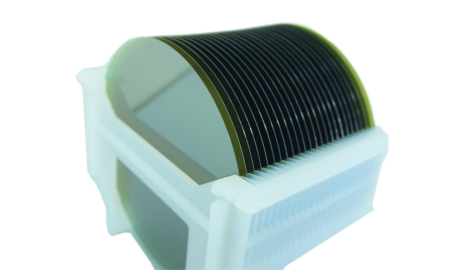
6-Inch SiC Conductive Type Substrate Single Wafer Specification |
||||
|
Grade |
Industrial Grade (P Grade) |
Test Grade (Grade D) |
Accompanying film grade (NG grade) |
|
|
Crystal parameters |
||||
|
Surface orientation |
4.0°toward<11-20>±0.50 |
NA |
||
|
Effective area (4H crystal form area) |
100% |
|||
|
Effective area(CS920) |
≥98% |
≥90% |
<90% |
|
|
Mechanical parameters |
||||
|
Diameter(mm) |
150±0.2 |
<149.8or>150.2 |
||
|
Main reference plane orientation |
<10-10>±5.0° |
NA |
||
|
Main reference plane length(mm) |
47.5±2.0 |
<45.5or>49.5 |
||
|
Secondary reference surface |
Without |
|||
|
Edge removal |
3mm |
|||
|
Thickness(μm) |
350±25 |
300~325or>375 |
<300 |
|
|
TTV(μm) |
≤10 |
≤15 |
>15 |
|
|
LTVave(μm) |
≤1 |
≤3 |
>3 |
|
|
LTVmax(μm) |
≤3 |
≤5 |
>5 |
|
|
Bow(μm) |
-25~25 |
-45~45 |
<-45or>45 |
|
|
Warp(μm) |
≤45 |
≤80 |
>80 |
|
|
S-plane roughness(nm) |
<0.3 |
NA |
||
|
Electrical parameters |
||||
|
Resistivity (Q · cm) |
0.015~0.025 |
0.015~0.028 |
0.015~0.03 |
|
|
Dopant |
N-type nitrogen doping |
|||
|
Defect parameter |
||||
|
Hexagonal inclusion (Intense Light/Microscope/CS920) |
Without |
Yes. |
||
|
Carbon wrap density(a/cm2) |
≤0.1 |
≤0.5 |
>0.5 |
|
|
Base plane dislocationBPD |
≤3000 |
≤9000 |
>9000 |
|
|
Spiral Dislocation TSD |
≤200 |
≤1000 |
>1000 |
|
|
Blade dislocation TED |
≤3000 |
≤7000 |
>7000 |
|
|
Microtubule density(个/cm2) |
≤0.5 |
>0.5 |
||
|
Front quality(Si surface) |
||||
|
Si surface treatment |
Si surface CMP |
|||
|
Crack (strong light) |
Without |
Yes. |
||
|
Scratches (strong light) |
Without |
Yes. |
||
|
Pit (strong light) |
Without |
Yes. |
||
|
Knock edge (strong light) |
Without |
Yes. |
||
|
Edge collapse(mm) (Microscope) |
length<0.5,depth<0.2 |
NA |
||
|
Missing edge(mm) (Microscope) |
Without |
Yes. |
||
|
Hexagonal hole (strong light) |
Without |
Yes. |
||
|
Si surface particle aggregation (CS920) |
Without |
Yes. |
||
|
% of scratches (CS920) |
≤5% |
>5% |
||
|
Scratch cumulative length (mm)(CS920) |
Cumulative length≤100 |
Cumulative length<300 |
Cumulative length>300 |
|
|
Stacking fault(CS920) |
≤1% |
>1% |
NA |
|
|
pit(a)(CS920) |
≤20 |
≤100 |
>100 |
|
|
Back quality(C side) |
||||
|
Back treatment |
C-side polishing |
|||
|
Back scratches (strong light) |
Visually no scratches |
NA |
||
|
Back roughness |
<1nm |
|||
|
Laser marking on the back |
Single line marking, length from main side1mm,Distance from both sides (main side endpoint perpendicular)12-15mm,Laser lettering depth0-10μm |
|||
|
Broken edge (strong light) |
Without |
Yes. |
||
|
Edge profile |
||||
|
Edge profile |
Chamfering |
|||
|
Packaging |
||||
|
Packaging |
Multi-piece or single-piece packaging, ready to use |
|||
 Home
Home
 Product
 News
News
 Contact